Custom chips shift OpenAI and SpaceX off Nvidia
OpenAI's Jalapeño chip, built with Broadcom, is a hedge against single-supplier risk rather than a break with Nvidia: it targets the inference workloads that now dominate compute spend, while general-purpose GPUs keep the training tasks. Google, Apple, and SpaceX are making the same bet on hardware tuned to their own workloads. What custom silicon buys is memory bandwidth and lower latency per token; what it costs is a design locked to today's model shapes.
What Custom AI Chips Actually Optimize
Defining Custom AI Chips and Hardware Optimization
Specialized silicon executes set neural network operations with greater efficiency than general-purpose graphics processors. Unlike GPUs built for broad compatibility, these units eliminate unused logic gates to reduce latency and power consumption per token. This architectural focus addresses an industry shift where inference workloads now dominate over model training, demanding hardware tuned to specific needs rather than flexible compute. Nvidia currently controls the dominant share of the high-end AI chip market, creating single-supplier risk for substantial infrastructure operators.
Nvidia Dominance Versus the Custom Chip Market
Infrastructure planners face a stark choice: accept the flexibility of merchant silicon or chase the performance gains of dedicated hardware. Developing custom silicon requires substantial upfront capital and lengthy design cycles that many enterprises cannot absorb. You must balance immediate deployment needs against long-term operational efficiency gains. Does your inference volume justify the engineering investment required to bypass standard architectures? Customization offers control while introducing complex supply chain management responsibilities previously handled by vendors.
Early adopters report latency reductions in specific serving scenarios. Design cycles often span 12 to 18 months before first silicon arrives. Initial fabrication batches carry failure rates that require careful validation protocols. Organizations need clear metrics to justify the shift from established GPU fleets.
Inside the Architecture of Specialized Silicon Design
ASIC Inference Architecture vs General GPU Cores
Custom inference chips strip away unused logic gates to optimize specifically for LLM Workloads. General-purpose GPUs keep flexible scheduling units built for rendering and diverse training tasks, which introduces latency penalties during steady-state token generation. ASICs remove these overheads by hardwiring the matrix multiplication paths required for transformer blocks. Companies integrating HBM3e directly into custom architectures achieve 2x the memory-to-core throughput compared to standard PCIe-connected GPUs. This bandwidth advantage lets designers bypass the NVLink Fusion bottlenecks that constrain general-purpose clusters.
| Feature | General GPU Cores | ASIC Inference Architecture |
|---|---|---|
| Logic Scope | Broad (Training, Rendering) | Narrow (Inference Only) |
| Memory Path | PCIe / NVLink | Integrated HBM3e |
| Scheduling | Flexible Context Switching | Static Pipeline |
| Efficiency | Moderate | High |
The design process removes floating-point units unnecessary for quantized inference, reducing power density per operation. Such specialization creates a rigid dependency on the target model family because architectural shifts in the algorithm may require a full silicon respin. Builders must weigh the throughput gains against the risk of obsolescence before committing to fabrication. Maximum efficiency arrives with a heavy constraint on flexibility.
Mechanics: OpenAI Jalapeño Deployment with Broadcom Partnership
OpenAI transitions from hardware consumer to co-designer through its partnership with Broadcom, unveiled in June 2026 to produce the Jalapeño inference chip. This collaboration removes general-purpose logic gates found in standard GPUs, hardwiring matrix multiplication paths specifically for transformer blocks. Unlike training accelerators that prioritize massive throughput, inference chips optimize for memory bandwidth and low-latency token generation. The design places HBM3e memory directly alongside the compute cores instead of behind a PCIe link. Such bandwidth optimization bypasses the interconnect bottlenecks that typically constrain steady-state token generation speeds.
The shift allows the company to avoid the expensive grip of single-supplier dominance while tuning silicon to exact model parameters. Massive upfront capital is required for this approach, which locks the architecture to current model shapes and limits flexibility for future algorithmic shifts. Engineers must weigh the performance gains against the risk of stranded assets if model architectures diverge from the hardcoded design. Unlike off-the-shelf solutions, custom silicon demands continuous co-engineering between software teams and fabrication partners to remain viable. This dependency creates a tight feedback loop where hardware updates must match software iteration cycles precisely.
The hidden tension lies in the opportunity cost of engineering cycles. Custom chips offer superior inference performance, yet diverting talent from algorithm development to hardware co-design slows overall model iteration. Nvidia's massive valuation reflects its ability to absorb R&D costs that would cripple smaller competitors. Consequently, the market bifurcates into generalists relying on merchant silicon and giants owning their stack. Builders must assess whether their inference volume justifies the multi-year investment required to exit the merchant supply chain. Only organizations with steady-state token generation at scale can amortize the non-recurring engineering expenses effectively.
Measurable ROI and Performance Gains from Dedicated Hardware
Defining Measurable ROI in Custom Silicon Deployments
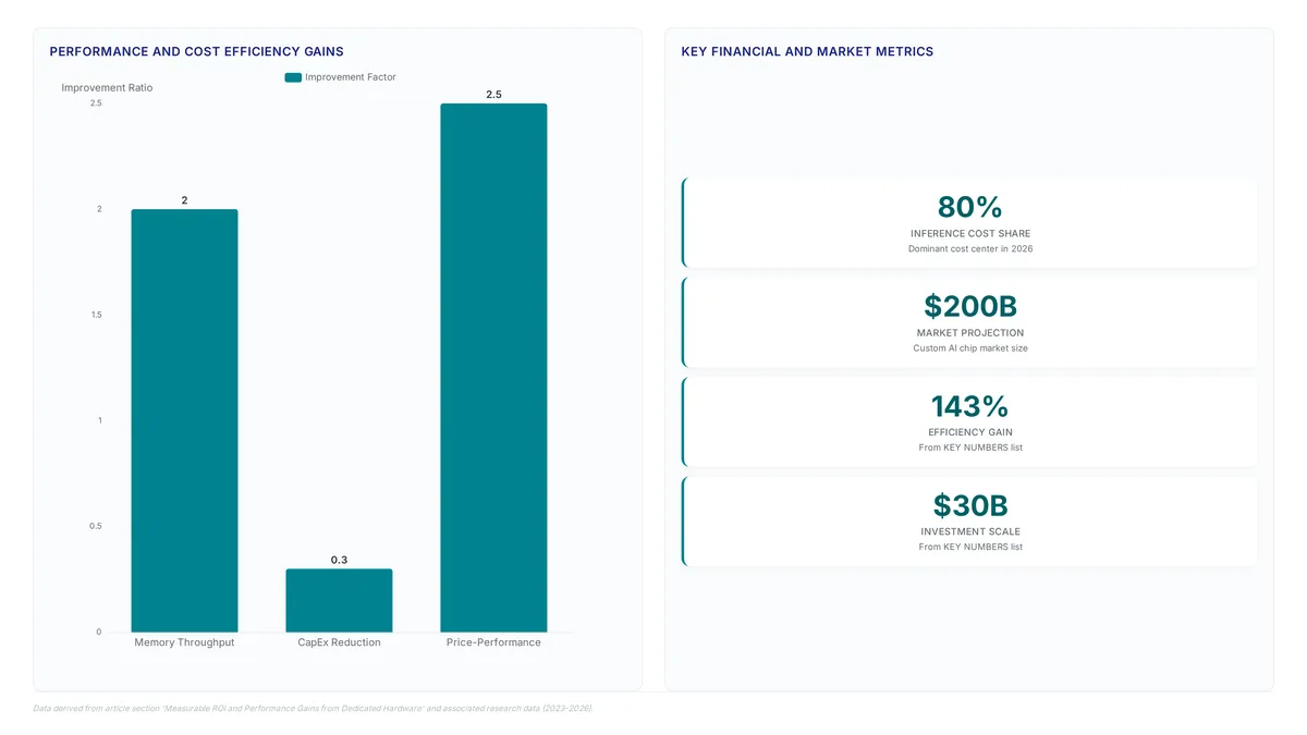
Measurable ROI in custom silicon extends beyond raw throughput to include supply chain hedging and workload-specific efficiency gains. This strategy directly addresses the primary driver for custom development: the need to slash costs associated with renting or purchasing expensive standard hardware.
Technically, return on investment is quantified by memory-to-core throughput improvements rather than simple clock speeds. These efficiency gains lower the total cost of ownership, which is critical as inference workloads become the dominant cost center in 2026. However, this approach requires significant upfront engineering investment and lacks the universal software compatibility of established GPU ecosystems. For builders, the metric for success is not replacing all existing hardware but optimizing the marginal cost per token for specific, stable models. The financial justification relies on balancing reduced operational expenditure against the fixed costs of design and validation.
Mitigating Single-Supplier Risk Through Hardware Diversification
Relying on a single vendor for critical compute capacity creates a fragile supply chain vulnerable to allocation bottlenecks. This move joins Google, Apple, and SpaceX in an expanding list of companies building their way out of single-supplier risk. Rather than attempting a complete hardware replacement, most organizations are adopting heterogeneous deployments that balance general-purpose GPUs with specialized inference silicon. This architectural split allows operators to hedge against market dominance while retaining access to established ecosystems for broad training tasks.
Implementation: Strategic Hedging Against Single-Supplier Risk in AI Hardware
Execute a heterogeneous deployment to mitigate single-supplier risk while maintaining baseline compute capacity. This strategy involves retaining Nvidia GPUs for general training tasks while offloading high-volume inference to custom silicon. The goal is less of a clean break and more of a hedge against market concentration.
- Map inference bottlenecks to justify the non-recurring engineering costs inherent in ASIC development.
- Define a narrow instruction set that excludes general-purpose graphics functions unnecessary for specific model architectures.
- Partner with foundries like Broadcom to design custom inference accelerators.
OpenAI transitioned from a hardware consumer to a co-designer by partnering with Broadcom to unveil LLM-optimized inference chips in June 2026. This Jalapeño project illustrates the execution path for organizations seeking custom silicon without owning a foundry.
About
Priya Nair serves as AI Industry Editor at AI Agents News, where she tracks the business dynamics shaping autonomous agent infrastructure. Her daily work analyzing product launches and platform shifts for companies like OpenAI and Cursor provides the perfect vantage point to dissect the strategic pivot toward custom AI chips. As substantial players from SpaceX to Google move to mitigate single-supplier risk, Nair's expertise in verifying market moves ensures a clear-eyed view of this hardware evolution. At AI Agents News, her team focuses on the frameworks and systems engineers use to build, making the underlying compute layer a critical beat. This article connects her rigorous coverage of agent platforms to the hardware reality powering them, explaining why controlling silicon is becoming as vital as optimizing orchestration logic for technical leaders evaluating the future of multi-agent systems.
Conclusion
Scaling custom silicon introduces a hidden operational tax: the inability to pivot when model architectures shift. While general GPUs absorb algorithmic changes, ASICs lock organizations into specific computational patterns, creating a rigidity that can stall innovation if the underlying math evolves. This is not merely a hardware choice but a bet on architectural stasis. Companies must recognize that the path to efficiency often leads to a fragmented infrastructure where managing dual-architecture clusters becomes the primary bottleneck. The initial capital savings from specialization frequently erode under the weight of maintaining separate software stacks and cooling requirements for legacy fixed-function logic.
Organizations should pursue custom chips only when steady-state inference volume is large and stable enough to amortize the non-recurring engineering expenses. Anything less is a premature commitment that trades future agility for marginal latency gains. The market dominance of established players creates a gravitational pull toward standardization that is difficult to resist without massive, sustained volume.
Start by running a side-by-side latency audit comparing your current most-used model variant against a simulated fixed-function pipeline using open-source emulation tools. This data-driven approach reveals whether your specific traffic patterns truly justify the loss of flexibility before you engage in costly non-recurring engineering discussions.
Frequently Asked Questions
Single-supplier dependence exposes operators to allocation bottlenecks when one vendor controls critical compute capacity. That fragility is why most companies keep Nvidia for broad training tasks and move high-volume inference to their own accelerators.
Custom chips remove unused logic gates to reduce latency significantly. This architectural focus allows companies to achieve double the memory-to-core throughput compared to standard GPUs, optimizing hardware for specific batch sizes and context windows.
Major firms like OpenAI, Google, and Apple are engineering proprietary silicon.
The Jalapeño chip optimizes for low-latency token generation rather than training. Unlike general-purpose GPUs, it eliminates overhead to serve large language models efficiently, addressing the specific constraints found in high-volume inference deployments.
Builders exchange flexibility for significant efficiency gains in power and speed. While this approach secures supply chains, it locks operators into specific model families, requiring heavy upfront engineering investment for long-term operational savings.
References